INTRODUCTION
A Solar PV inverter is an electrical device that changes the direct current (DC) electricity, which is produced by Solar PV panels, into alternating current (AC).
A micro inverter converts direct current (DC) from a single solar panel to alternating current (AC).
NEED OF MICRO INVERTER
The present use of micro inverters is mostly restricted to commercial production of electricity to be supplied to the electrical grid. Using these inverters in residential areas is costly because these inverters are costly themselves. Experts in the field of solar energy have estimated that the demand for micro inverters would quadruple by the end of 2017. According to records, every year our nation suffers a huge loss due to shortage of electricity. Although most of the nation has a sufficient supply of electricity, however there are areas which are still deficit of electricity. Some areas have supply for only few hours in the day.
PROPOSED MODEL
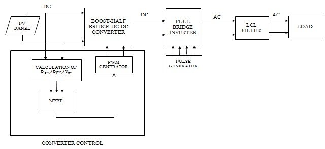
This is the proposed model of solar based microinverter.
We will get 12-24 V DC voltage (depending on the solar panel) from panel.
The problem is the maximum available power from the solar PV cannot be extracted during light load requirement. Furthermore, when the load requirement is higher than the maximum available power from the Solar PV (especially during the night time), this kind of systems cannot work. Hence, one storage system needs to be placed which can act as a buffer for the excess or the deficit amount of power resulted from the mismatch of the maximum power available from the solar PV and load power requirement. As the PV module comes in parallel to the DC link load, PV voltage and the load voltage are inevitably same. Hence, the converter is unable to perform load voltage regulation. The MPP voltage which is same as that of the load voltage changes with a change in radiation and temperature. The MPPT controller gives the reference load voltage or the reference inductor current command.
Then there is Inverter(DC/AC) stage which convert boosted DC voltage to AC voltage.Pulse (PWM signals) is provided to Inverter stage to drive the MOSFET(which I will discuss further)
Then output AC needs to filter by filter circuit and finally it is given to load.
P.S : I worked on the Inverter stage only.
INVERTER STAGE
Basically I came across to two circuits “Half Bridge Inverter circuit” and “Full Bridge Inverter circuit”.
The main difference between half bridge and full bridge inverter is the maximum value of output voltage. In half bridge inverter, peak voltage is half of the DC supply voltage. In full bridge inverter, peak voltage is same as the DC supply voltage.(You will get more when we will come to working)
WORKING OF HALF BRIDGE INVERTER CIRCUIT
1.This type of Inverter requires two power electronics switches (MOSFET). The MOSFET or IGBT is used for switching purpose.
2.A single DC source is divided into two DC Sources.
3. Initially, two MOSFETs are not triggered to turn ‘ON’, so zero current flows through the device.
4. The MOSFET 1 is turned ‘ON’ by giving a gate pulse it. The MOSFET 2 is kept ‘OFF’ and no gate signal is given to it.
5. Thus, the MOSFET 1 starts conducting and the current starts to flow from Vdc/2(positive terminal of 1st source)Load-negative terminal of 1st source.
6. Thus, a positive cycle similar to that of ac cycle is obtained.
7. Now, the MOSFET 1 is made ‘OFF’ and MOSFET 2 is made ‘ON’ by giving a gate signal to it.
8. The MOSFET 2 starts to conduct and the current starts to flow through the load.
9. Thus, a negative cycle is produced.Two SCRs are triggered alternatively so that the load conducts current in both directions.Thus, a square ac wave is generated.Hence, direct current is converted into alternating current using inverter circuit.
P.S : Theory seems good to hear but the major issue is switching of MOSFET s and to drive the gate terminal of MOSFET with the pulse. We can’t just give pulse of 50 Hz to drive the gate terminal. I have used Decade counter(4017) to drive the gate terminal and it was not capable enough to drive the gate terminal and then I did some research and I came to know of Driving ICs. There are plenty of driving IC’s IR2110, SG3525,etc. I decided to use IR2110 as it was available and referred to datasheet
IR2110 Datasheet: https://www.infineon.com/dgdl/Infineon-IR2110-DataSheet-v01_00-EN.pdf?fileId=5546d462533600a4015355c80333167e
IR2110 Inverter Circuit
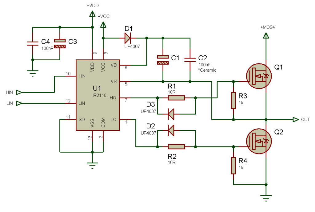
The operation of this circuit is based on the microcontroller programming which is used to provide signals for the gate driver circuitry. The microcontroller board used in the circuit is Arduino UNO. The Arduino is programmed for generating PWM signal for the input logic pins of the IR-2110 IC.
void setup() {
// initialize digital pin 2 and 3 as an output.
pinMode(3, OUTPUT); // at Hin pin of Ir2110 IC
pinMode(7, OUTPUT); // at Lin pin of Ir2110 IC}
// the loop function runs over and over again forever
void loop() {
//initially 2 and 3 pin are low
digitalWrite(7, HIGH); // Lin pin high
delay(10); // wait for 10ms second
digitalWrite(7, LOW); // Lin pin low
delayMicroseconds(1); // dead time of 1us
digitalWrite(3, HIGH); // Hin pin high
delay(10); // wait for 10m second
digitalWrite(3, LOW); // Hin pin LOW
delayMicroseconds(1); // dead time of 1us
}
For driving the high side MOSFET, the IR2110 is used along with the bootstrap circuitry. For input logic signal at Lin and Hin pin, two square waves of 180-degree phase difference are applied as both the MOSFETs should not turn on at the same time. In such a situation the MOSFETs can get damaged due to short circuiting at the output. As shown in the figure above the MOSFET Q1 is in high side configuration and MOSFET Q2 is in the low side configuration. Let us now understand how this circuit drives both high and low side MOSFET. For turning ON the MOSFET the Vgs should be greater than the threshold voltage (Vth) of the MOSFET. That means, Vgs = Vg – Vs>Vth
In this circuit, IRF840 MOSFET are used. These have a threshold voltage (Vth) in range from 10V to 12V. So the Vcc is equal to 12V and the threshold voltage is also 12V. When Hin is low and Lin is high so the transistor Q2 turns ON without any external circuit ( as Vg-Vs = 12 – 0 = 12V ) and transistor Q1 is OFF, it can be said that the low side MOSFET is ON in this case. Therefore the diode D1 is forward bias and the capacitor C3 starts charging from point a to b up to 12V through transistor Q2 and a low voltage is obtained at the output
In the next cycle when Hin is high and Lin is low then transitor Q2 turns OFF and transistor Q1 turns ON. That means the high side MOSFET is ON in this case.
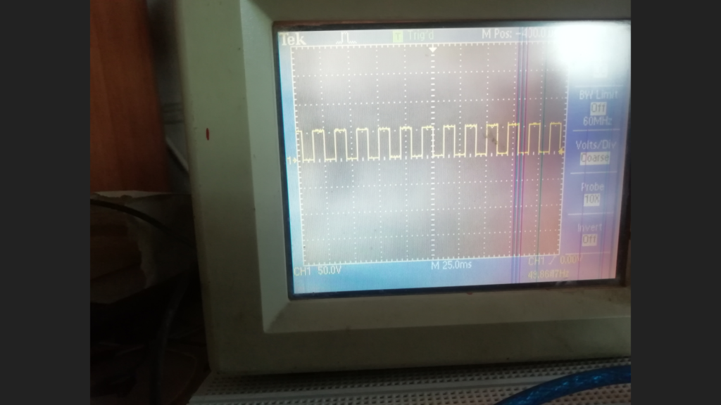
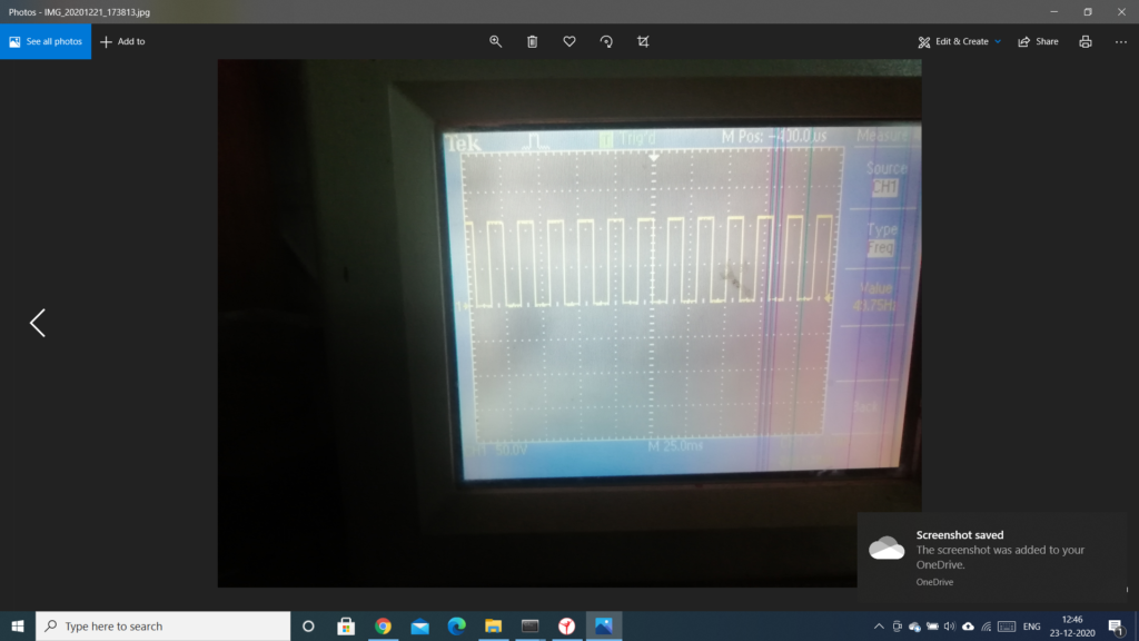
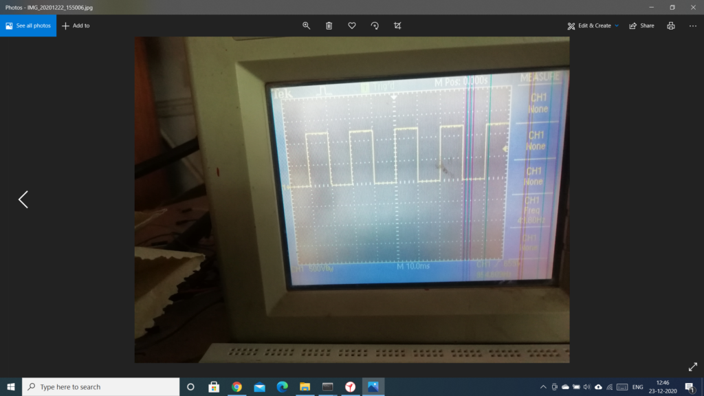
Below are images of Input and the Output through Arduino, IR2110, and the total circuit


Video link for IR2110 Half Bridge Inverter
https://drive.google.com/file/d/1GZnEkCy6Wyp3xVcMxmJqBUtbAHPP7Stc/view?usp=sharing